From GDSII to Wafer: EDA Design Flow and Data Conversion for Wafer-Scale Manufacturing of Superconducting Quantum Chips
From GDSII to Wafer: EDA Design Flow and Data Conversion for Wafer-Scale Manufacturing of Superconducting Quantum Chips
Ling Qiao, Fumin Luo, Qinglang Guo
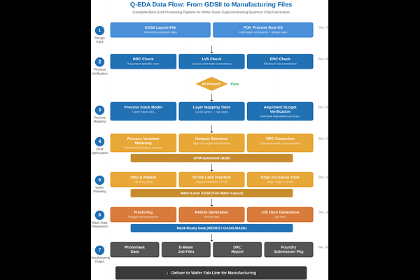
AbstractSuperconducting quantum computing is advancing toward the thousand- and even million-qubit regime, making wafer-scale fabrication an essential pathway for achieving large-scale, cost-effective quantum processors. This manufacturing paradigm imposes new requirements on quantum-chip electronic design automation (Q-EDA): design tools must not only generate layouts (GDSII files) that satisfy quantum-circuit physical constraints but also ensure that the design data can be seamlessly converted into a complete set of manufacturing files executable by a wafer foundry, thereby enabling reliable translation from design intent to physical chip. This paper focuses on this critical data-conversion pipeline and presents a systematic treatment of the Q-EDA technology stack for wafer-scale fabrication. Starting from GDSII as the single authoritative data source, we analyze the key stages including process-design-kit (PDK)-based design rule checking (DRC), layout-versus-schematic (LVS) verification, design for manufacturability (DFM) optimization, wafer layout planning, and mask data preparation (MDP). We describe the concrete architecture of a Q-EDA system, present nine quantum-specific DRC rules together with their physical underpinnings and a multi-layer process stack model, and benchmark the manufacturing data-flow coverage of mainstream Q-EDA tools. Finally, we discuss the core challenges and future directions in this field.